SoC Software Design Tools
The SoC FPAA includes a toolset for system design where a user of Okika’s FPAAs can easily compile their design in a process that starts with a description of the IC and ends with the programming of the FPAA. Compilation starts with using a range of high-level block abstractions, followed by a literal list of FG switches (and intermediate representations like Verilog), mapped to each individual measured performance parameters in each FPAA. The SoC tool set is open-source and to explicitly enable a wider user community for mixed-signal configurable designs. The tool integrates a high-level design environment built in Scilab and Xcos (an open-source clone for MATLAB and Simulink, respectively), with a compilation tool, x2c, to compile from high level description to a targetable switch list to be programmed on the FPAA device.

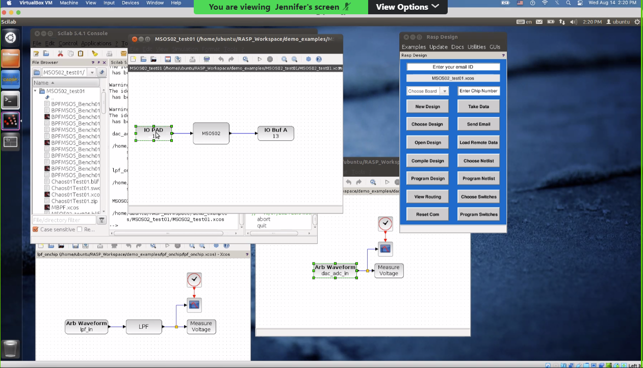
An example of the SoC design tools is shown in the following sequence with a low pass filter computation. The user chooses basic design options through the FPAA tools GUI, which starts running when the Scilab tools are started in the Ubuntu Virtual Machine (VM). The FPAA device details are specified in architecture files for analog–digital SoC. The graphical high-level tool uses a palette for available blocks that compile down to a combination of digital and analog hardware blocks, as well as software blocks on the resulting processor.

Using the Xcos palette for FPAA blocks shown below, the user can select from four sections, namely Analog, Digital, Input/Output and Complex Blocks. The Analog, Digital and I/O blocks consist of basic elements in different tiles of a chip. Complex Blocks are pre-defined circuit blocks made of more than one basic element.

Shown below are simulation results for 4 input and output computation. Lines, and resulting blocks, allow for vectorized as well as scalar inputs. Inset shows the Xcos diagram and user sets parameters for simulation or for compiling into the FPAA.

The result of this example design in the SoC tool chain is shown below for a 1 input and output computation.

The tools output a single programming file, that is a combination of multiple smaller files compressed into a single structure, that is used for floating gate programming and SRAM memory setup for the SoC FPAA. The design tools can process the downloading of this file, as well as other devices (e.g. remote computer, tablet). The SoC FPAA devices now enable floating gate device programming entirely on the device as an input data stream, therefore the entire data stream, including µP code to execute programming, simply looks like a single stream of data to the system. The FPAA utilizes a 16-bit MSP430 microprocessor (µP), embedded 16k × 16 SRAM for program and data memory, as well as the memory mapped registers for programming.