An analog-to-digital converter can only digitize the signal presented at its input. It cannot recover information that was clipped, buried in noise, distorted by improper loading, or corrupted by aliasing before conversion. This is why the performance of a data-acquisition system often depends as much on the analog signal-conditioning stage as it does on the ADC itself.
Signal conditioning prepares a real-world analog signal for conversion. Depending on the application, this may include amplification, attenuation, filtering, level shifting, buffering, differential conversion, protection, or calibration. The goal is not merely to match the ADC’s input- range, but is to preserve the integrity of the signal and deliver clean, stable, low noise input that enables the ADC to capture the maximum amount of useful information accurately.
Start with the signal, not the circuit
Before selecting amplifiers or filters, or ADCs, define the characteristics of the signal you need to measure and the performance required from the measurement system. At minimum, document:
-
The minimum resolvable signal and maximum input amplitude
-
frequency range of interest
-
The expected common-mode voltage or DC offset
-
The source impedance and its variation with frequency or operating conditions
-
The noise and interference environment
-
The ADC input range, sampling rate, reference requirements and input structure
-
The required accuracy, system level resolution, and response time
These values determine what the analog front end must accomplish. A thermocouple producing millivolt-level changes needs a different signal chain from a vibration sensor with a wide dynamic range. A slowly changing bridge sensor may prioritize low noise, offset and drift, while an ultrasonic system may prioritize bandwidth and settling time.
The ADC is equally important. Many converters have switched-capacitor or sample-and-hold inputs that require rapid charge transfer during acquisition. A source that appears adequate under DC conditions may not drive the ADC input or settle to the required accuracy within the acquisition time. The required front end must therefore be designed around both the sensor characteristics and the ADC’s dynamic input requirements..
Use gain to make better use of the ADC range
An ADC makes the best use of its available resolution when the input signal spans as much of its input range as possible without clipping.
A small signal that occupies only a fraction of the ADC input range uses only a fraction of the available output codes. Digital multiplication after conversion can increase the numerical value, but it cannot recover measurement resolution that was not captured during conversion.
Consider a sensor that produces a 20 mV full-scale output connected to an ADC with a 0 V to 3.3 V input range. The sensor signal would use only about 0.6% of the ADC’s full scale range. An analog gain stage can expand the signal before conversion, allowing the useful measurement to occupy more codes.
The highest possible gain is not always the correct choice. The design must leave margin for:
-
Sensor tolerance and overload conditions
-
DC offset and drift
-
Noise peaks
-
Amplifier output swing limits
-
ADC input overvoltage limits
-
Transient events during startup or mode changes
Gain should be distributed carefully when several stages are used. Applying gain early can improve the signal relative to the noise of later stages, but excessive front end gain can cause saturation if significant offsets or interference are present. The correct gain plan balances resolution, headroom, and stability across the complete signal chain.
Filter before conversion
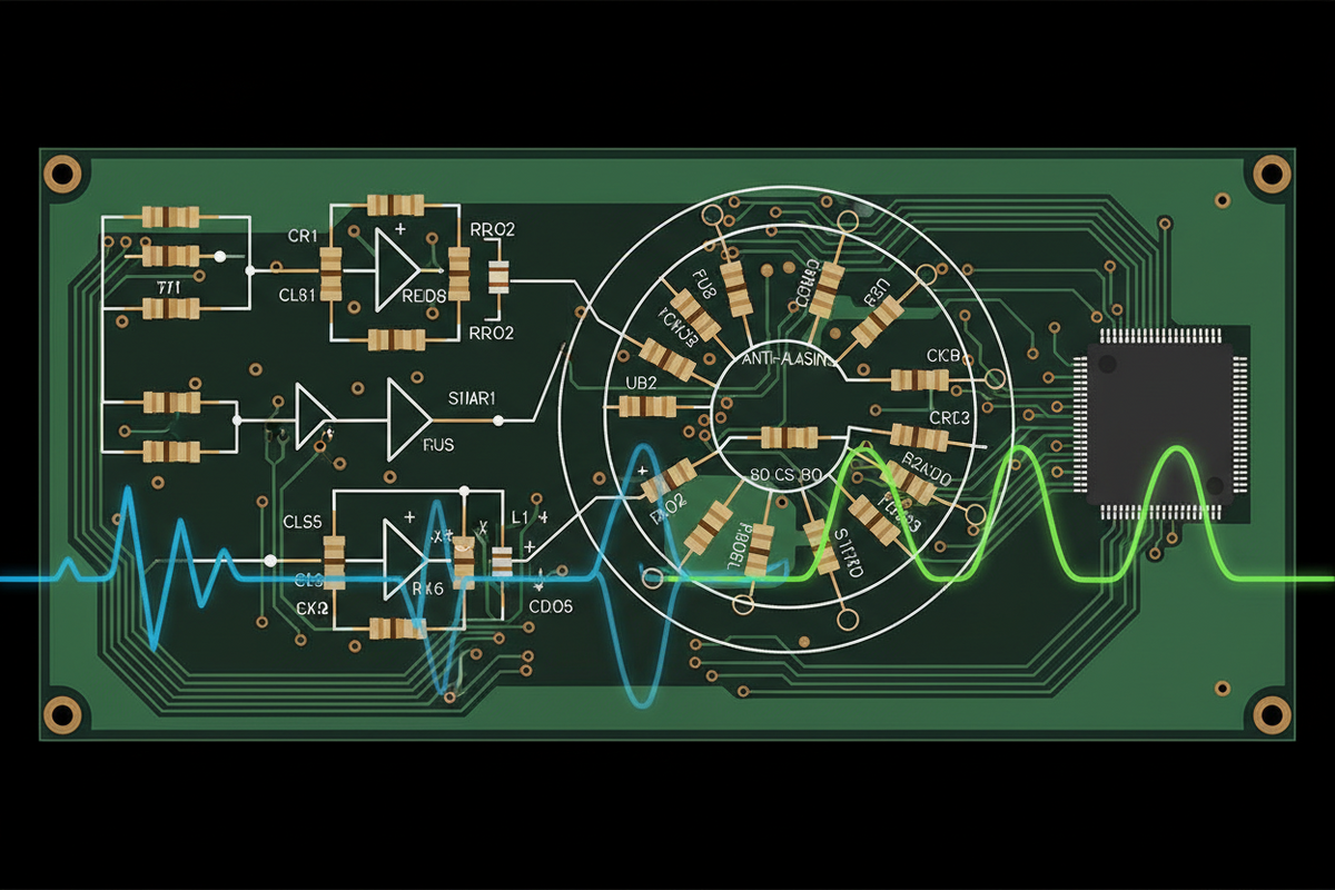
Filtering serves two related purposes. It reduces noise outside the band of interest, and it attenuates frequencies that could alias into the measured band when the signal is sampled.
Once an out-of-band signal aliases into the digital data, it is indistinguishable from a real in-band signal. A digital filter after the ADC cannot reliably separate the two. For that reason, data-acquisition systems commonly include an analog low-pass or band-pass filter before conversion.
The filter should be designed around the actual signal bandwidth and sampling plan. Important questions include:
-
What is the highest frequency that must be preserved?
-
What unwanted frequencies are present?
-
How much attenuation is required at the Nyquist frequency?
-
How much phase shift or group-delay variation can the application tolerate?
-
How quickly must the system respond to steps or transients?
Sampling substantially faster than the minimum required rate can simplify the analog filter design. A higher sampling rate increases the frequency separation between the signal band and frequencies that can alias into it, providing a wider transition band over which the analog filter can attenuate unwanted signals.
A simple RC filter may be sufficient for a slow sensor with a high sampling ratio. A higher-order active or programmable filter may be necessary when the passband is close to the Nyquist limit, when strong interference is nearby, or when the operating bandwidth changes between modes.
Shift and center the signal correctly
Many sensors produce signals that swing above and below 0 V, while many embedded ADCs accept only positive input voltages. A signal centered around 0 V may need to be shifted to a midpoint such as 1.65 V before entering a 0 V to 3.3 V input range. The gain and offset should leave sufficient headroom for signal excursions, tolerances, noise, and overload conditions.
Level shifting is more than adding a DC offset. The reference used to create that offset must be stable and sufficiently low noise. Its impedance must also be compatible with the amplifier and ADC. A noisy midpoint reference can appear directly in the conversion results.
Differential ADCs introduce additional considerations. The signal must fit within both the differential input range and the permitted common-mode range. Fully differential amplifiers or differential signal-conditioning stages can translate a single-ended sensor signal into the format the ADC expects while controlling the output common-mode voltage.
A robust design checks the voltage at every internal node under minimum, nominal, and maximum conditions. This analysis should include sensor tolerances, offsets, gain errors, supply variation, and expected signal extremes. This prevents a circuit from appearing correct in simulation while clipping under real sensor tolerances or power-supply variation.
Manage source impedance and acquisition settling
An ADC input is not always a high-impedance, passive load. In many successive-approximation converters (SAR) , the input drives an internal sampling capacitor through a switching network. During the acquisition period, the external source must charge that capacitor and allow the input to settle to within the error required by the system’s resolution and accuracy target.
High source impedance can cause incomplete settling, gain errors, distortion, or channel-to-channel interaction in multiplexed systems. A buffer amplifier may be needed to isolate the sensor or filter from the ADC input. The buffer must be selected for the required bandwidth, noise, output drive, stability, and settling behavior.
The resistor-capacitor network placed between the driver and ADC also matters. A small capacitor near the ADC can supply charge during sampling, while a series resistor can isolate the amplifier from the capacitive load. However, values that are too large may slow settling or create unwanted attenuation. The interface should be simulated and validated using the converter’s acquisition timing and input model whenever possible.
Multiplexed ADCs can impose additional settling requirements. When the input switches between channels at significantly different voltages, residual charge from the previous channel can affect the next acquisition. Adequate acquisition time, low source impedance, buffering, or, in some cases, discarding the first conversion after a channel change may be necessary.
The interface should be analyzed using the ADC's specified acquisition time, sampling capacitance, and input model whenever possible. Simulation is useful, but the design should also be validated under worst-case source impedance, channel voltage changes, sampling rate, and operating conditions.
Choose single-ended or differential signaling intentionally
Single-ended circuits are simpler, but they reference the signal to a shared ground. Ground noise, voltage drops, and external interference can therefore become part of the measurement, particularly when the signal source and ADC are physically separated or do not share exactly the same ground potential.
Differential signaling measures the difference between two conductors and can reject noise that appears equally on both. This can be valuable for low-level sensors, long cable runs, industrial environments, and systems with multiple power domains. Differential signals can also provide a natural interface to many high-performance ADCs designed for differential inputs.
The amount of rejection achieved depends on the common-mode rejection ratio of the complete signal path and on how well the two sides are balanced. Mismatched source impedances, routing, filter components, or amplifier behavior can convert common-mode noise into differential error and reduce the expected benefit.. Differential signal conditioning should be treated as a complete balanced path rather than two unrelated single-ended circuits.
The common-mode voltage must also remain within the permitted range of the amplifiers and ADC throughout normal operation and expected transients. Differential signaling can tolerate some difference in ground potential between the source and receiver, but it does not provide galvanic isolation. If the ground-potential difference can exceed the allowable common-mode or input-voltage range, an isolation strategy may be required.
Differential signaling is not always necessary. For short PCB connections, relatively large signals, and systems with a clean, well-controlled shared ground, a single-ended interface may provide adequate performance with less complexity. Differential signal paths can require additional amplifiers, matched components, routing effort, board area, and power. The choice should therefore be based on the required noise immunity, signal level, grounding environment, and ADC interface rather than on an assumption that differential signaling is inherently better.
Add protection without compromising the measurement
Real sensor inputs may be exposed to electrostatic discharge, wiring errors, overvoltage, or transient events. Input protection can include series resistance, clamps, transient suppressors, current limiting, or dedicated protection devices. The appropriate network depends on the expected fault conditions and the sensitivity of the measurement.
Protection components can introduce capacitance, leakage current, noise, and nonlinearity. A clamp diode that is acceptable for a general-purpose input, for example, may create unacceptable leakage in a high-impedance sensor interface. Added capacitance can also interact with source impedance or filtering and affect settling time.
The protection design should distinguish between the ADC's normal input range and its absolute-maximum ratings. Staying within the absolute-maximum ratings may prevent permanent damage, but it does not guarantee correct conversion or normal operation. The signal-conditioning circuit should keep the ADC within its specified operating range during normal measurements while ensuring that fault conditions do not exceed safe voltage or current limits.
Clamp-current paths also require attention. Protection diodes that conduct into a supply rail can raise or disturb that rail, particularly when the system is unpowered or the rail cannot absorb current. Series resistance or dedicated protection devices may be needed to limit fault current, and the complete current path should be evaluated rather than considering only the voltage at the ADC pin.
The protection network should be selected for both survivability and measurement performance. Leakage, capacitance, noise, bandwidth, settling behavior, fault energy, and recovery after an overload should all be considered when selecting and placing protection components.
When a reconfigurable analog front end makes sense
A fixed analog circuit is often the best choice when the signal range, filter response, and operating conditions are stable. A reconfigurable analog front end becomes more attractive when the system must support several sensors, bandwidths, gain ranges, or operating modes.
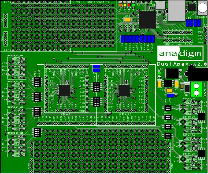
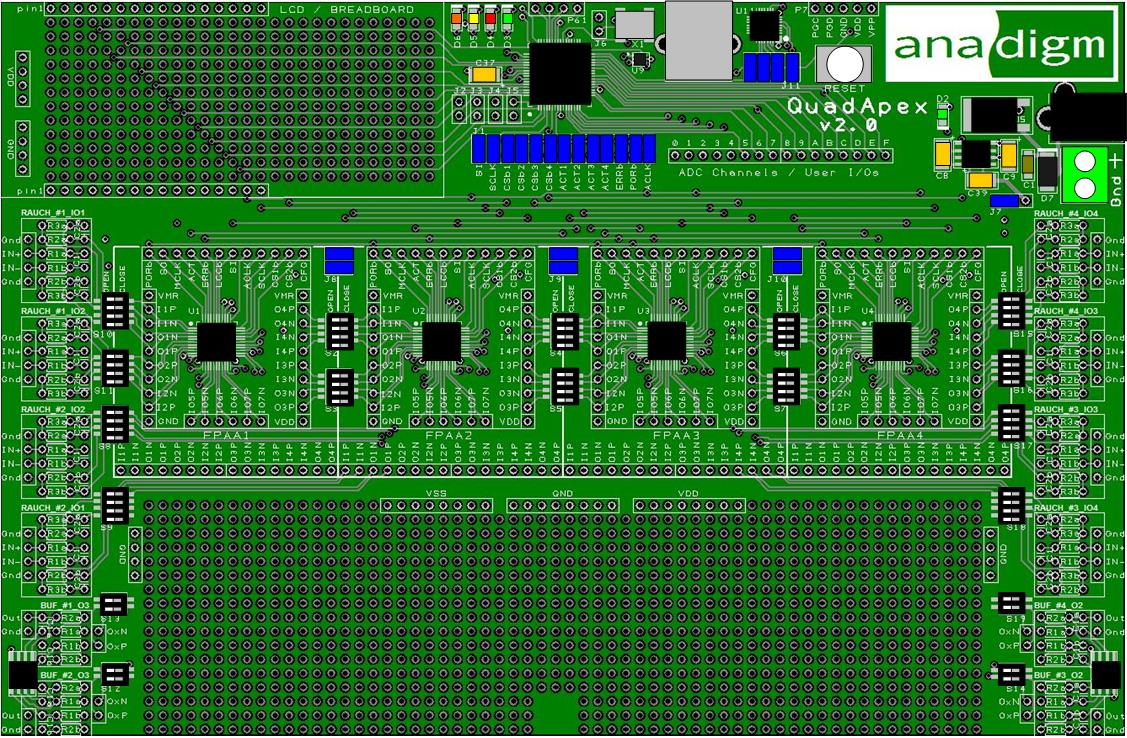
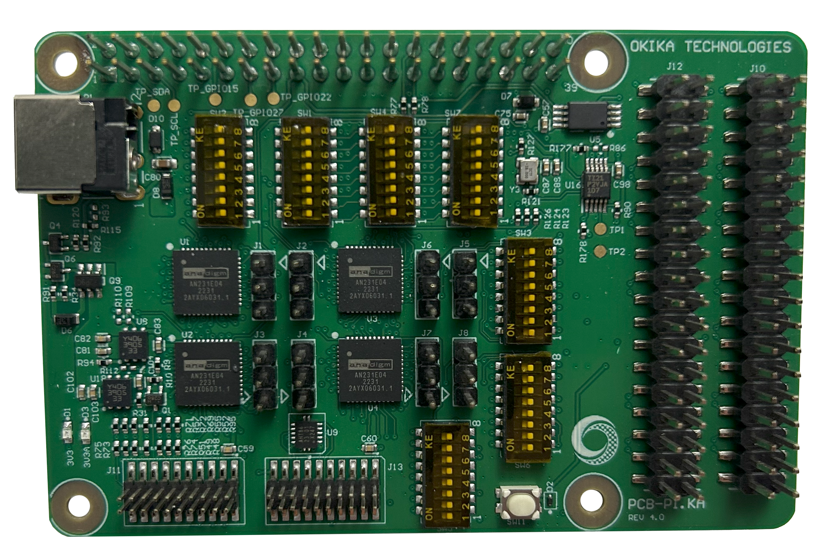
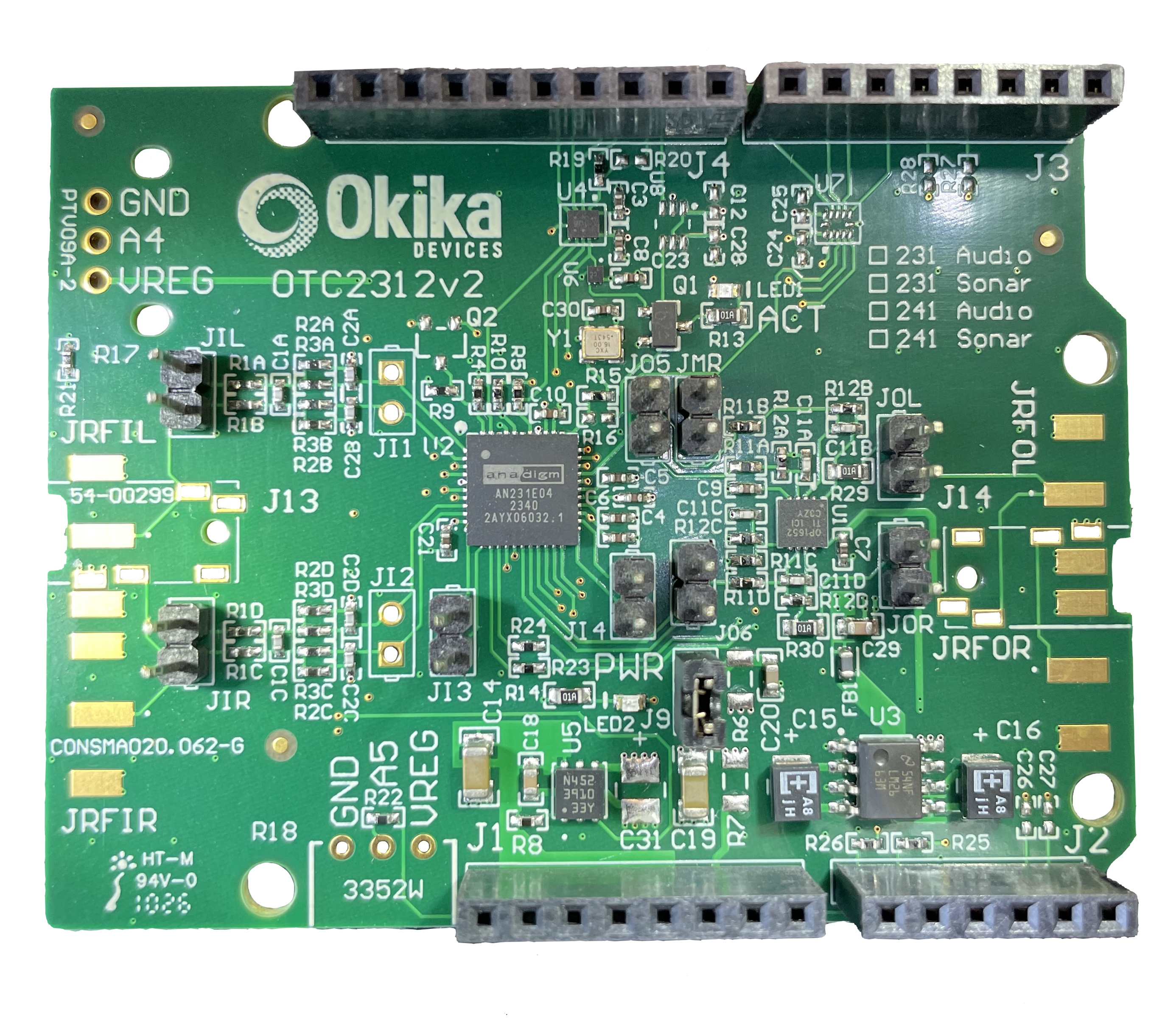
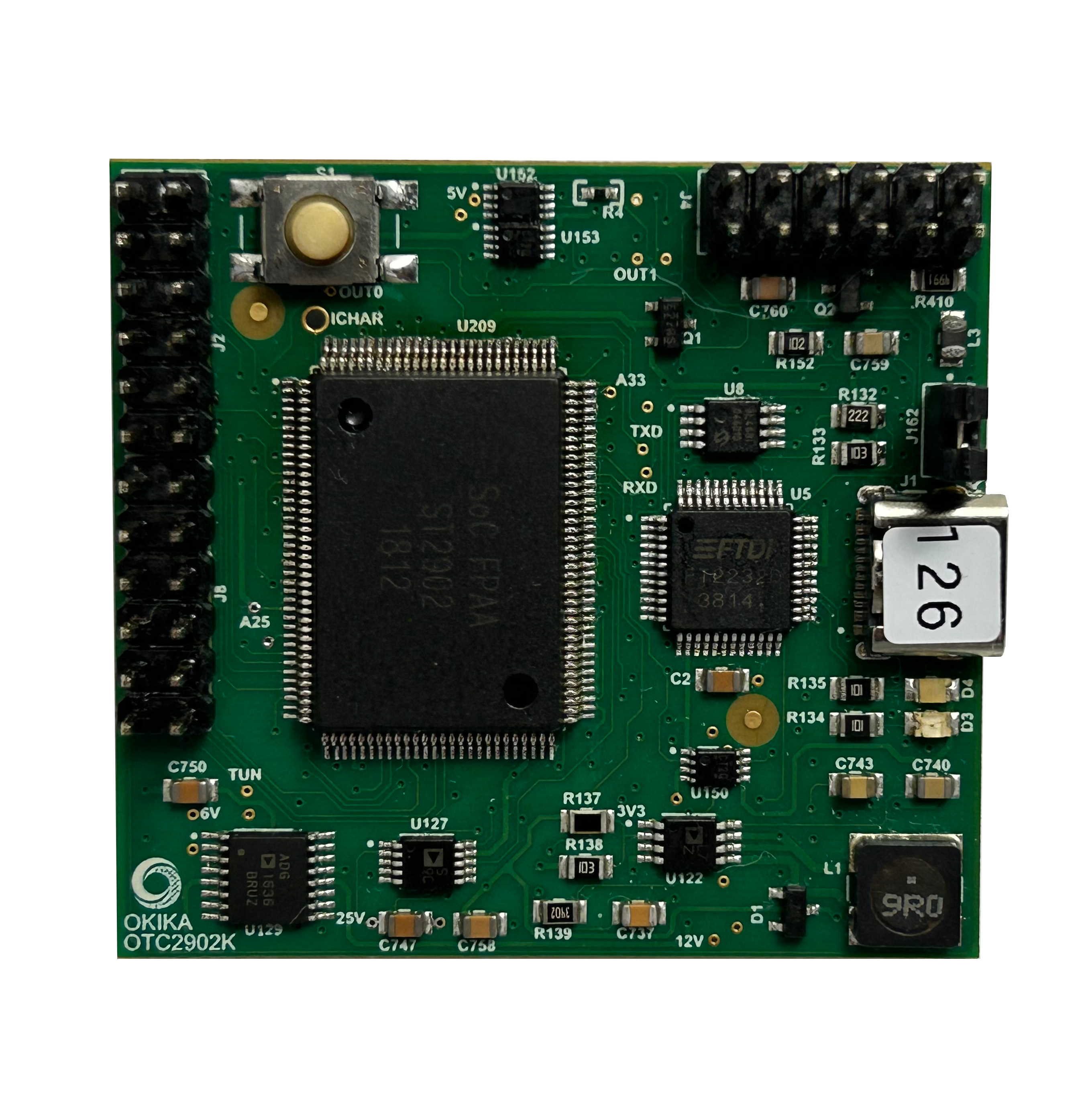
A field-programmable analog array (FPAA) can implement functions such as gain, filtering, comparison, integration, and routing in configurable analog hardware. The signal is still processed in the analog domain before conversion, but the circuit behavior can be adjusted through configuration data rather than a PCB redesign.
This approach can be useful when engineers need to:
-
Change gain as the sensor range or operating conditions changes
-
Switch between filter bandwidths or responses
-
Reuse one hardware platform across several product variants
-
Calibrate or compensate the analog path in software
-
Update the signal chain after deployment
-
Prototype and evaluate several analog architectures on the same hardware
Reconfigurability does not remove the need for analog engineering. Headroom, noise, bandwidth, grounding, stability and ADC drive requirements still apply. It changes how the circuit is implemented and how quickly its behavior can be revised.
The primary advantage is not that programmable analog eliminates conventional signal-chain design, but that it allows the implementation to be adapted without changing the physical hardware. This can be particularly valuable when requirements evolve, several measurement modes must share one platform, or the optimal analog configuration depends on operating conditions.
A practical signal-conditioning checklist
Before releasing a sensor-to-ADC design, verify the following:
-
The maximum expected signal including tolerance, offset, noise, and overload margin, does not clip any amplifier or exceed the ADC’s permitted input range.
-
The useful signal range occupies enough of the ADC range to meet the required resolution and accuracy.
-
The analog bandwidth preserves the required signal while limiting unwanted noise and interference.Anti-alias attenuation is sufficient for the selected sample rate and signal bandwidth
-
The ADC driver settles to the required accuracy within the available acquisition time.
-
Source and load impedances are compatible throughout the signal chain
-
Differential and common-mode voltages remain within the specified ranges of the amplifiers and ADC.
-
Noise, offset, and drift from amplifiers, resistors, references, and supplies of other components fits within the system error budget.
-
Protection components do not introduce excessive leakage, noise, capacitance, or settling errors during normal operation.
-
Bench testing includes gain, offset accuracy, frequency response, noise, clipping, settling, channel switching and relevant temperature or supply variation.
-
The ADC reference and any bias or midpoint references meet the required accuracy, noise, impedance, and stability requirements.
-
Multiplexed inputs have sufficient settling time after channel changes, particularly when channels can differ significantly in voltage.
-
Expected fault and transient conditions do not exceed component voltage, current, power, or absolute-maximum ratings.
-
Configuration or gain changes allow sufficient settling time before subsequent ADC samples are treated as valid.
The design should be verified not only under nominal conditions but also across worst-case component tolerances, sensor extremes, supply limits, temperature range, and relevant operating modes. A signal chain that performs correctly at nominal values may fail to meet its accuracy, headroom, settling, or protection requirements at the limits of real-world operation.
Better conversion begins before the converter
Selecting a higher-resolution ADC does not automatically create a higher-resolution system, stable resolution, dynamic range, noise, and accuracy depends on the performance of the complete signal chain. The analog front end plays a critical role by determining the quality of the signal presented to the converter.
By treating gain, filtering, level shifting, impedance, and protection as a coordinated signal-conditioning problem, engineers can make better use of the converter’s capabilities and produce cleaner, more accurate, and more predictable measurements. Good ADC performance begins with ensuring that the signal arriving at the converter is already in the right range, bandwidth, and electrical form.
When requirements are likely to change, programmable analog hardware can add flexibility while keeping essential functions such as gain, filtering, and level translation in the analog domain before conversion. This allows the signal chain to adapt to different sensors or operating conditions without giving up the advantages of conditioning the signal before information can be lost through clipping, noise,or aliasing.