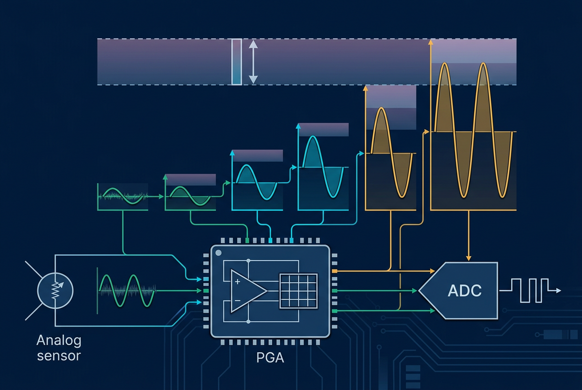
A sensor can produce a small signal in one operating condition and a much larger signal in another. Fixed gain that protects the largest signal may leave the smallest signal using only a fraction of the ADC range. Programmable gain lets the system choose a better range, provided every setting leaves enough headroom and samples taken during transitions are handled correctly.
Consider a vibration sensor with nominal output peaks of 20 mV, 80 mV, and 250 mV in three operating modes. We will select gains for a 12-bit, 0–3.3 V ADC, account for nonideal behavior, and determine what must happen when the gain changes.
For the wider signal-chain requirements, see Analog Signal Conditioning Before the ADC. This example focuses on gain selection. All numerical limits below are design assumptions and calculated results, not measured performance or specifications for an Okika board.
Define the sensor and output limits
Assume the sensor has already been buffered or interfaced appropriately and its nominal signal is centered around zero. A level-shifting output stage places the amplified waveform around 1.65 V at the ADC input. All gains in this example are end-to-end voltage gains from that sensor signal to the ADC input.
The output window is narrower than the ADC’s nominal range because an amplifier may lose linearity before reaching a supply rail. Its permitted swing depends on load, supply, temperature, and common-mode voltage. Use guaranteed operating limits where available, not absolute maximum ratings.
The ±1 mV noise allowance is a chosen excursion budget, not an RMS value or a guarantee that random noise has a hard maximum. A real design must define its noise bandwidth, statistical assumptions, observation time, and acceptable overload probability. Impulsive interference needs its own allowance.
Calculate the maximum gain with headroom included
The available excursion from the nominal center to either output limit is:
For nominal sensor peak amplitude , a conservative input envelope is:
The 25% allowance covers larger-than-nominal signal peaks. The remaining terms reserve room for input-referred offset and noise. All quantities are in volts. We add worst-case magnitudes rather than combining them by root-sum-square because this is a clipping check.
Including gain error and the output-referred budget, a nominal gain must satisfy:
Therefore:
For the smallest signal, , the maximum nominal gain is approximately 45.35. Select the largest available setting below that limit: 32 V/V.
Repeat the calculation for the other modes:
All three calculated envelopes remain inside 0.20–3.10 V. A gain of 16 is too large for the medium mode; a gain of 8 is too large for the high mode.
For example, in high-amplitude mode:
The ADC input can therefore extend 1.31674 V in either direction from its nominal 1.65 V center, under the stated budget. This leaves about 133 mV to each usable output limit.
Check what the gain buys at the ADC
An ideal 12-bit ADC with a 3.3 V span has an LSB size of:
Using the nominal signal amplitudes, without adding the reserved error margins:
If the system used fixed gain of 4 for every mode, the low-amplitude signal would span only 0.16 V, or approximately 199 code intervals. Selecting gain of 32 expands that span by eight times, equivalent to three bits of code utilization.
That is not a promise of three additional effective bits. Gain also amplifies sensor noise and input offset, and the amplifier contributes its own errors. The benefit is strongest when ADC quantization or downstream noise limits the measurement. More gain cannot improve the sensor’s own signal-to-noise ratio.
After settling, recover sensor amplitude using the calibrated gain and zero offset for the active setting. Record the gain with the samples. Otherwise, a range change can look like a change in the physical quantity being measured.
Check every analog stage for clipping
The calculation above protects the final output under the assumed limits. It does not prove that every internal node remains linear.
If gain is distributed among an input amplifier, filter stages, and an ADC driver, check the swing and common-mode range at each stage. Include filter peaking and large out-of-band signals. A later attenuator cannot repair clipping that has already occurred earlier in the chain.
The same applies to offset correction. Subtracting an offset digitally can improve the reported zero, but it cannot restore analog headroom lost before conversion. If the sensor’s DC offset is too large, use suitable analog offset cancellation or AC coupling when the application permits it. AC coupling would change this example’s DC response.
For an FPAA implementation, the assumed 1.65 V ADC center is not automatically the FPAA’s internal reference. Translate signal levels as required by the device and board. Okika’s FlexAnalog interfacing guide explains the differential, reference-centered signal path and external interfacing options.
Choose who controls the gain
A programmable gain amplifier provides a controllable gain element. It does not necessarily include the detector, thresholds, and control loop required for automatic gain control. An AGC system also needs decisions about peak versus RMS detection, attack time, release time, hysteresis, and overload recovery.
For this sensor, start at low gain when the amplitude is unknown. Increase gain only after enough observation to establish that the next setting leaves the required headroom. Use different up-range and down-range criteria, plus a minimum hold time, to avoid repeated switching near a threshold.
When a larger operating mode is known in advance, lower the gain before that mode starts. A sudden 250 mV peak arriving while gain is 32 demands an output excursion far beyond this circuit’s limits. An AGC loop reacting afterward cannot guarantee preservation of the first unexpected peak.
For amplitude measurements, scheduled or block-by-block range selection may be preferable to continuously moving gain. AGC changes the signal envelope; reconstructing the original amplitude requires valid samples and a known, calibrated gain history.
Wait for the analog path before accepting samples
A successful register write or configuration transfer establishes a control state. It does not establish that the analog output has settled.
After a gain change, consider amplifier settling, switching transients, filter state, ADC acquisition settling, and any converter pipeline or digital-filter memory. Settling depends on the error band as well as the size and direction of the transition. The PGA281 datasheet, for example, lists settling under specified gains, voltage steps, and accuracy limits; those numbers should not be applied to a different signal chain unchanged.
To see the scale of the problem, suppose an illustrative downstream first-order low-pass has a 2 kHz pole. For a 2.9 V step, its ideal residual error is an exponential decay with a time constant of about 79.6 µs. Reaching half an LSB of this 12-bit ADC, approximately 0.403 mV, takes:
At 20 kS/s, this spans about 14.1 sample periods. An implementation could conservatively reserve 15 periods, or 750 µs, after the actual gain update for this ideal filter alone. This is an illustrative settling model, not a specified blanking time, an anti-aliasing design, or a complete 12-bit accuracy budget.
The actual chain may take longer, especially after overload or with a higher-order filter. Its accepted samples must correspond to acquisition intervals after the validated settling deadline, not simply to conversion results read after that deadline. ADC driver and input-network behavior also matter.
A practical transition sequence is:
-
Mark the affected data invalid and command the new gain.
-
Identify when the new analog configuration becomes active.
-
Wait for the validated worst-case settling interval and required ADC acquisition time.
-
Flush any conversion pipeline or digital-filter history affected by the transition.
-
Resume valid data with the new gain identifier and calibration coefficients.
Decide whether a dedicated PGA is enough
A dedicated PGA, or an ADC with an integrated PGA, is often sufficient when only gain needs to change. Choose it against the required input common-mode range, source impedance, gain accuracy, noise, bandwidth, output swing, and settling performance. An integrated PGA can simplify the interface, but its own input and gain-dependent limits still apply.
An FPAA becomes more useful when gain changes accompany other analog changes: narrowing bandwidth in a quiet monitoring mode, switching filter responses for different sensors, or routing a signal through alternative processing paths. Coordinating those functions can reduce the need for several separately controlled analog circuits.
That flexibility does not guarantee better noise or accuracy than a dedicated precision PGA. Check whether the requested gains are realizable, how they affect bandwidth and resource use, and whether the complete configuration meets the example’s ±1% gain and offset/noise budgets. Those budgets are requirements to verify, not assumed FPAA specifications.
Take the example to hardware
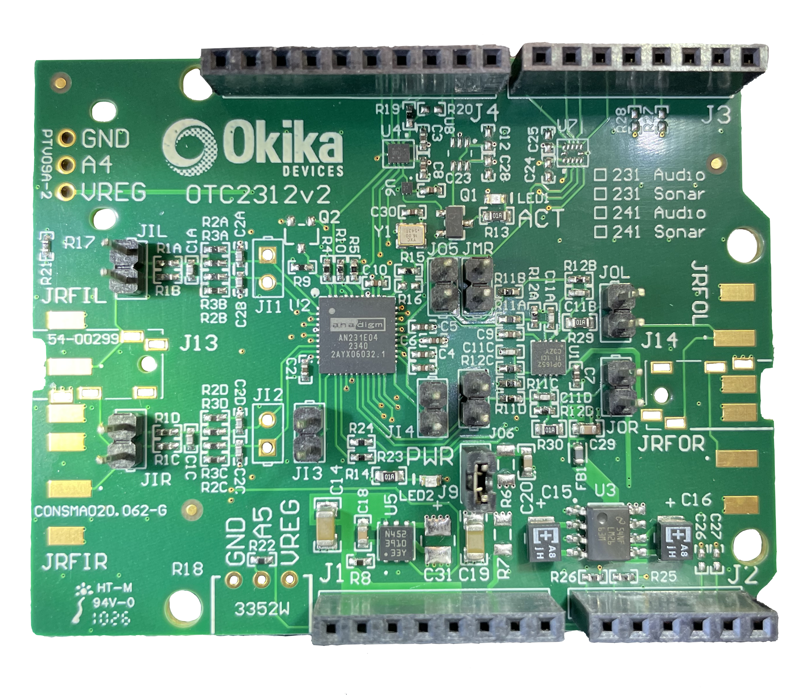
Use Arduino Analog Signal Conditioning: Build a Programmable Low-Pass Filter and Amplifier as the microcontroller implementation path. The OTC2312 FlexAnalog Arduino Shield supports SPI-controlled runtime reconfiguration and provides analog interface circuitry for evaluation.
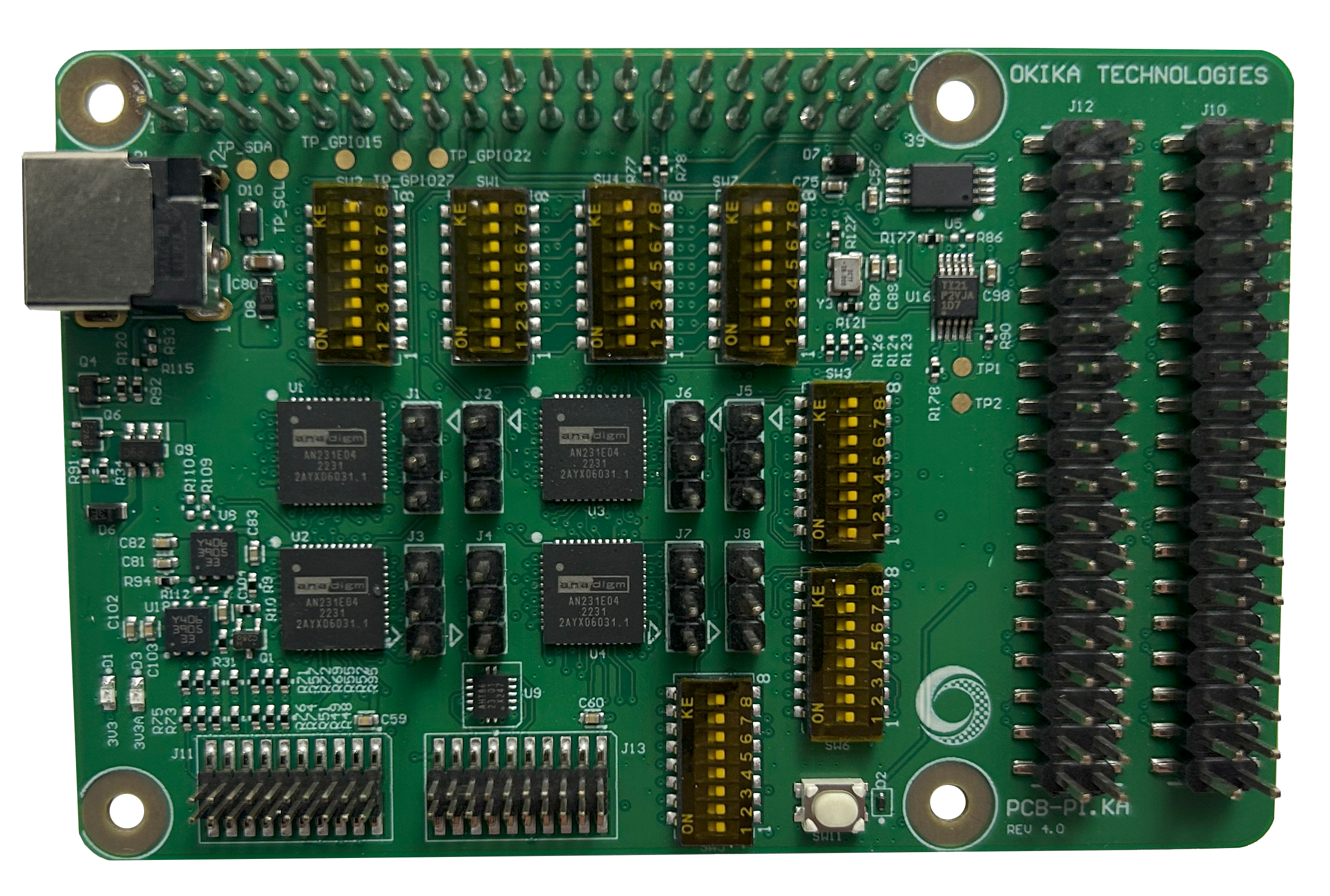
For host-controlled experiments and multiple analog paths, use the Raspberry Pi Analog Signal Conditioning article. The PIKA Raspberry Pi HAT provides four AN231E04 FPAAs and a host programming workflow.
Neither implementation path should be assumed to provide this example’s 12-bit, 0–3.3 V, 20 kS/s ADC behavior unchanged. Select a suitable converter and verify its electrical interface. Account for the board’s existing input/output gains and filters when translating the end-to-end gain targets.
On the bench, test all three amplitudes with the specified offsets and peak allowances. Measure actual gain, output extremes, noise, and distortion at every setting. Then test every gain-transition direction, including unexpected amplitude increases and overload recovery, to establish the earliest valid sample.
Next step: Open AnadigmDesigner2 and evaluate end-to-end gains of 4, 8, and 32 with the required filtering and interfaces. Validate the resulting design on the chosen board to confirm headroom, noise, and valid-sample timing.