
Choosing an anti-aliasing filter starts with four requirements: the signal bandwidth, the ADC sampling rate, the unwanted signal level, and the maximum alias error you can accept. Together, these determine how much attenuation the filter needs and how quickly its response must fall between the useful signal and unwanted frequencies.
Our Analog Signal Conditioning Before the ADC article covers the wider signal chain. Here, we work through a specific filter design, compare fourth- and eighth-order Butterworth responses, and translate the result into a Chameleon™ implementation candidate.
Start with a measurable specification
Consider a sensor acquisition system with the following requirements. The example assumes a SAR ADC sampling at the stated rate, followed by digital filtering that retains only the measurement band.
| Parameter | Example requirement |
|---|---|
| Useful signal bandwidth | DC to 5 kHz |
| ADC sampling rate | 40 kS/s |
| ADC Nyquist frequency | 20 kHz |
| Known interference | A 35 kHz sinusoid at 100 mV RMS at the analog filter input |
| Maximum residual alias from that interferer | 100 µV RMS, referred to the ADC input |
| Passband response target | No more than 0.1 dB variation from the low-frequency gain through 5 kHz |
| Nominal signal-chain gain | Unity |
| Attenuation design margin | 6 dB beyond the minimum requirement |
The 100 µV limit applies to this interference contribution. It is not a specification for total noise, offset, distortion, or overall measurement accuracy. Those need separate budgets.
Similarly, passband flatness describes how gain changes with frequency. Absolute gain accuracy and temperature drift must be specified separately.
Identify where the interference will alias
For a sinusoid, its alias frequency can be found from:
falias = |fin − kfs|
Choose the integer k that places the result between DC and fs / 2.
In this example:
|35 kHz − 40 kHz| = 5 kHz
The interferer folds directly onto the edge of the useful measurement band. A digital filter cannot remove it there without also affecting a legitimate 5 kHz signal.
This also explains why attenuation at Nyquist is not the only useful design criterion. With a retained bandwidth B = 5 kHz, the first positive-frequency band above Nyquist that folds into DC–5 kHz is:
fs − B through fs + B = 35–45 kHz
Higher bands around multiples of the sampling rate can also fold into the measurement band. Their interference and noise contributions must be evaluated too.
Using 35 kHz as the critical stopband frequency is appropriate for this example because the digital processing discards frequencies above 5 kHz. It does not mean the entire DC–20 kHz sampled spectrum is protected. If that full spectrum matters, the filter requirements change.
Convert the error limit into attenuation
For voltage amplitudes expressed on the same basis, the required attenuation is:
Arequired = 20 log10(Vinterference / Vallowed)
Therefore:
20 log10(100 mV RMS / 100 µV RMS) = 60 dB
The minimum is 60 dB at 35 kHz. Adding 6 dB of margin gives a nominal design target of 66 dB. At unity gain, 66 dB reduces the interferer to approximately 50 µV RMS.
If later stages add gain, include that gain when referring the error to the ADC input. For multiple interferers, allocate a combined error budget. Broadband noise requires integration of the filtered noise spectrum across the bands that alias into the measurement band; a single-tone calculation is not enough.
Choose the cutoff and filter order together
For an ideal unity-gain Butterworth low-pass filter, attenuation is:
A(f) = 10 log10[1 + (f / fc)2n]
Here, n is filter order and fc is the cutoff frequency. At the cutoff, attenuation is approximately 3.01 dB, regardless of order. Setting the cutoff equal to the highest useful signal frequency would therefore violate this example’s 0.1 dB passband target.
The passband requirement places a lower bound on cutoff:
fc ≥ fp / (10Ap/10 − 1)1/(2n)
The stopband requirement places an upper bound:
fc ≤ fstop / (10As/10 − 1)1/(2n)
Using fp = 5 kHz, Ap = 0.1 dB, fstop = 35 kHz, and As = 66 dB:
| Ideal Butterworth response | Minimum cutoff from passband target | Maximum cutoff from attenuation target | Feasible cutoff range? |
|---|---|---|---|
| Fourth order | 8.00 kHz | 5.24 kHz | No |
| Eighth order | 6.32 kHz | 13.54 kHz | Yes |
No cutoff allows the fourth-order Butterworth filter alone to meet both targets. An eighth-order response offers a workable range, including a standard 10 kHz cutoff. These bounds describe ideal filters; component tolerances and interface stages still need to be included.
Compare fourth- and eighth-order filters at 10 kHz
The following values are calculated from the ideal Butterworth equation. They are not measured Chameleon performance or guaranteed module specifications.
| Metric | Fourth order, 10 kHz cutoff | Eighth order, 10 kHz cutoff |
|---|---|---|
| Attenuation at 5 kHz | 0.0169 dB | 0.000066 dB |
| Attenuation at 10 kHz | 3.01 dB | 3.01 dB |
| Attenuation at 20 kHz | 24.10 dB | 48.16 dB |
| Attenuation at 35 kHz | 43.53 dB | 87.05 dB |
| Residual from the 100 mV RMS interferer | 666 µV RMS | 4.44 µV RMS |
| Meets the nominal 66 dB attenuation target? | No | Yes |
Both responses preserve the useful band in the ideal model. The difference is rejection: the fourth-order filter leaves an alias about 6.7 times larger than the allowed limit, while the eighth-order model provides substantial margin.
Higher order is not automatically the best choice. It is useful here because the required attenuation and available frequency separation justify it. Texas Instruments’ Active Low-Pass Filter Design discusses the response and implementation trade-offs among common filter families.
Trade sampling rate against filter complexity
Increasing the sampling rate creates more separation between the useful band and the first frequencies that can alias into it.
At 80 kS/s, the 35 kHz interferer remains outside the retained DC–5 kHz band and can be removed digitally, provided it does not overload or otherwise distort the analog chain. The first upper alias band now begins at 75 kHz.
A fourth-order Butterworth filter with a 10 kHz cutoff provides approximately 70 dB of ideal attenuation at 75 kHz. If a 100 mV RMS interferer were present there, that response would meet the same 66 dB design target. The actual interference spectrum must be reassessed whenever the sampling rate changes.
The trade-off is higher conversion throughput, potentially greater power consumption, and more digital processing. Digital filtering must precede any reduction in sample rate, or decimation can introduce new aliases.
For delta-sigma ADCs, use the converter’s modulator sampling and digital-filter characteristics to determine external filtering requirements. Its output data rate alone does not describe the complete aliasing behavior.
Include transient response in the decision
A Butterworth response provides a maximally flat magnitude characteristic, but it does not provide linear phase or guarantee an overshoot-free step response. Increasing order at a fixed cutoff generally increases delay and ringing.
The Chameleon datasheets list approximately 220 µs for the 10 kHz fourth-order module and 500 µs for the 10 kHz eighth-order module to settle within 1% following a 1 V step. These figures are not settling guarantees for a tighter error band.
For waveform capture, evaluate group delay and pulse shape. For control loops, include filter phase lag in the stability analysis. For multiplexed measurements, distinguish the filter’s response after an input change from the ADC driver’s settling during each acquisition interval.
Implement the design with Chameleon
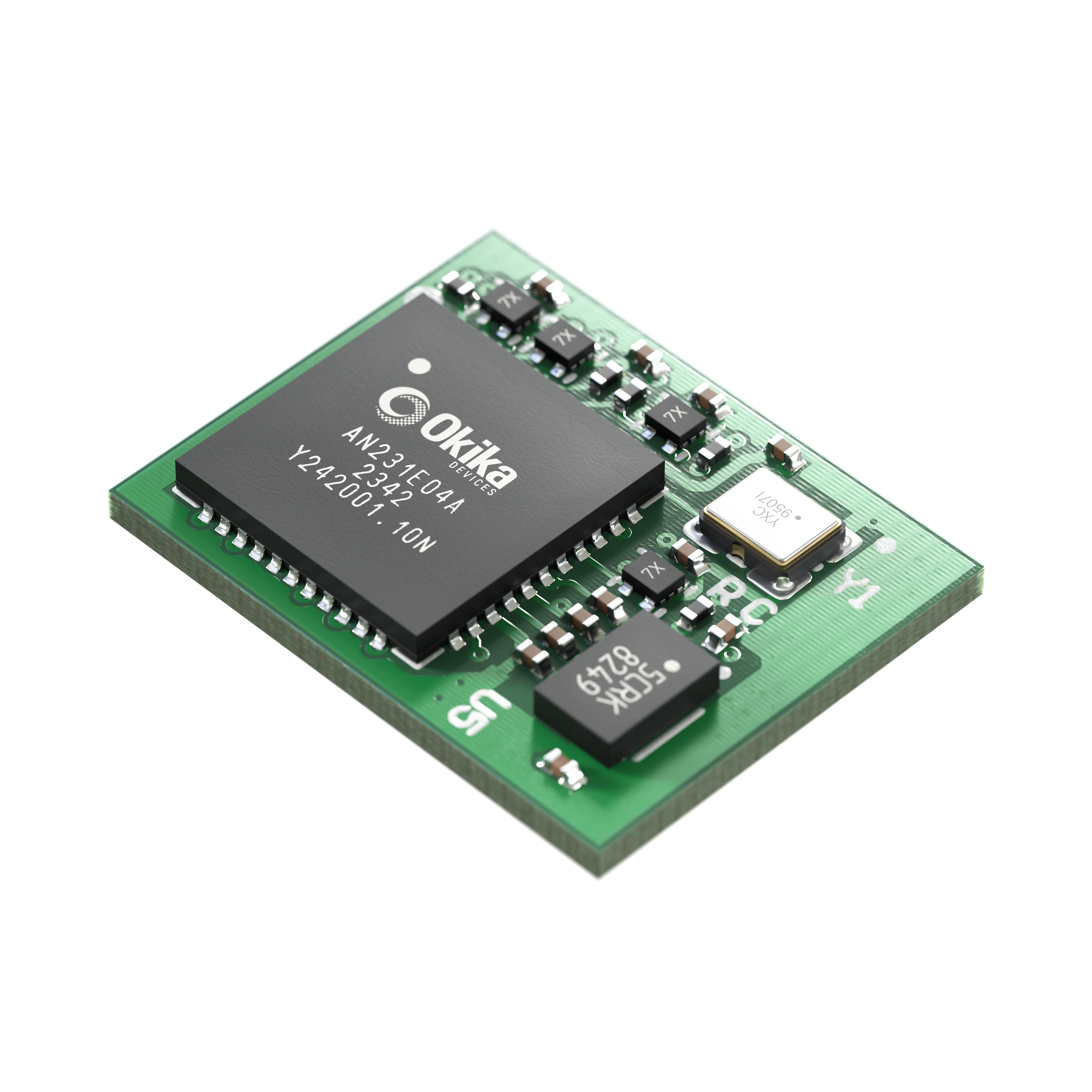
The Chameleon 8th Order Butterworth Lowpass Filter, OTC9314L, is the 10 kHz implementation candidate. It is supplied preconfigured; normal fixed-function operation does not require a programming board.
Use the OTC931xL datasheet for the circuit connections. A practical signal chain includes input conditioning, the module, output smoothing, and an ADC driver/interface network.
Filter before the switched-capacitor input
Chameleon’s core is a sampled analog circuit. High-frequency inputs can alias during that sampling operation, before the downstream ADC ever sees them. A continuous-time input filter must suppress relevant high-frequency energy. Its adequacy depends on the actual internal sampling configuration and interference spectrum, not only the ADC’s 40 kS/s rate.
For the 10 kHz module, the datasheet’s input Rauch network uses R1 = R2 = 10 kΩ, R3 = 4.7 kΩ, C1 = 1 nF, and C2 = 470 pF, with an approximately 23 kHz natural frequency and Q of 0.729. Follow its schematic; this is an active filter, not a single RC pole.
The input network also handles signal referencing. Preserve headroom for the useful signal plus the interferer before filtering has attenuated it. A correct small-signal response cannot prevent distortion caused by an overloaded input stage.
Suppress output clock feedthrough
The module provides an independent amplifier for a Rauch output-smoothing stage. Use that stage, with the datasheet topology as the starting point, to reduce switching artifacts before the ADC.
A nominal 23 kHz output stage is a reasonable candidate for this 5 kHz measurement band. Its required rejection must be checked against the measured clock-feedthrough spectrum and the ADC’s alias bands. If suppression is insufficient, revise the smoothing response or timing strategy.
Matched clocks can help control when sampling occurs, but synchronization does not automatically remove every spur or offset. Verify phase, settling, and residual artifacts in the assembled system.
Include both interface filters in the overall response calculation. Their transfer functions multiply, so gain changes add in decibels. Their extra poles do not make the complete cascade a twelfth-order Butterworth filter.
Design the final ADC interface
Select the driver and RC network for the ADC’s common-mode range, input swing, sampling capacitance, acquisition time, and settling target. Add a suitable buffer or differential driver where needed. A differential module output does not establish compatibility with every ADC.
The small network at the ADC pins must balance charge delivery, amplifier stability, and acquisition settling. Its values cannot be finalized from the filter cutoff alone. The interface guidance in Analog Signal Conditioning Before the ADC covers these checks.
Verify the complete signal chain
The calculated 87.05 dB rejection at 35 kHz establishes design intent. The module datasheet specifies 48 dB at twice cutoff; it does not guarantee the calculated 35 kHz result. Its listed 200 µV RMS wideband noise also uses stated test conditions with clock components removed. That figure must not be confused with the example’s 100 µV single-interferer allowance.
Before treating the design as qualified, verify:
- Passband response: Measure gain through 5 kHz, normalized to low-frequency gain, including both interface filters. Check absolute gain and drift separately.
- Interference rejection: Inject the 35 kHz, 100 mV RMS tone and measure its 5 kHz alias with no desired 5 kHz tone present. Confirm the residual is below 100 µV RMS.
- Other alias paths: Sweep relevant bands around ADC and filter sampling frequencies. Include expected higher-frequency interference and broadband noise.
- Clock artifacts and noise: Measure the assembled system with the intended clocks, supplies, layout, driver, and ADC operating together.
- Dynamic behavior: Test headroom, steps, overload recovery, acquisition settling, and operating extremes.
For this example, the specification is now concrete: preserve DC–5 kHz, limit passband variation to 0.1 dB, and achieve at least 60 dB rejection of the specified 35 kHz interferer, with a nominal 66 dB design target. An eighth-order Butterworth response at 10 kHz is a suitable starting point, subject to system verification.
Explore the Chameleon 8th Order Butterworth Lowpass Filter for the OTC9314L implementation, or compare the Chameleon 4th Order Butterworth Lowpass Filter when a higher sampling rate or a less demanding rejection target permits a lower-order response.
Technical references
- Okika Devices: OTC931xL 8th Order Butterworth Lowpass Filters datasheet, filter characteristics and interface circuits.
- Okika Devices: OTC932x Dual 4th Order Butterworth Lowpass Filters datasheet, filter characteristics and step settling.
- Texas Instruments: Active Low-Pass Filter Design, filter response and topology selection.
The worked-example values are analytical predictions for ideal responses. The implementation is a datasheet-based design candidate, not a bench-validated reference design.