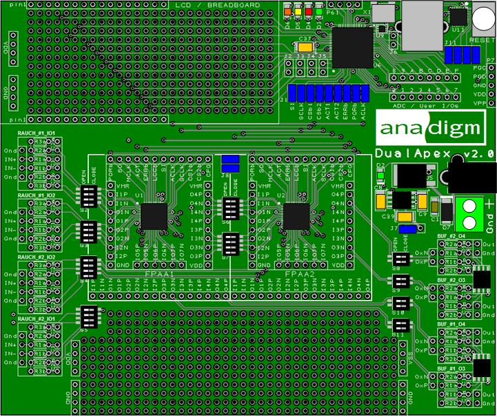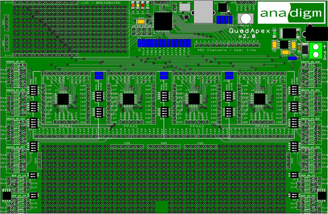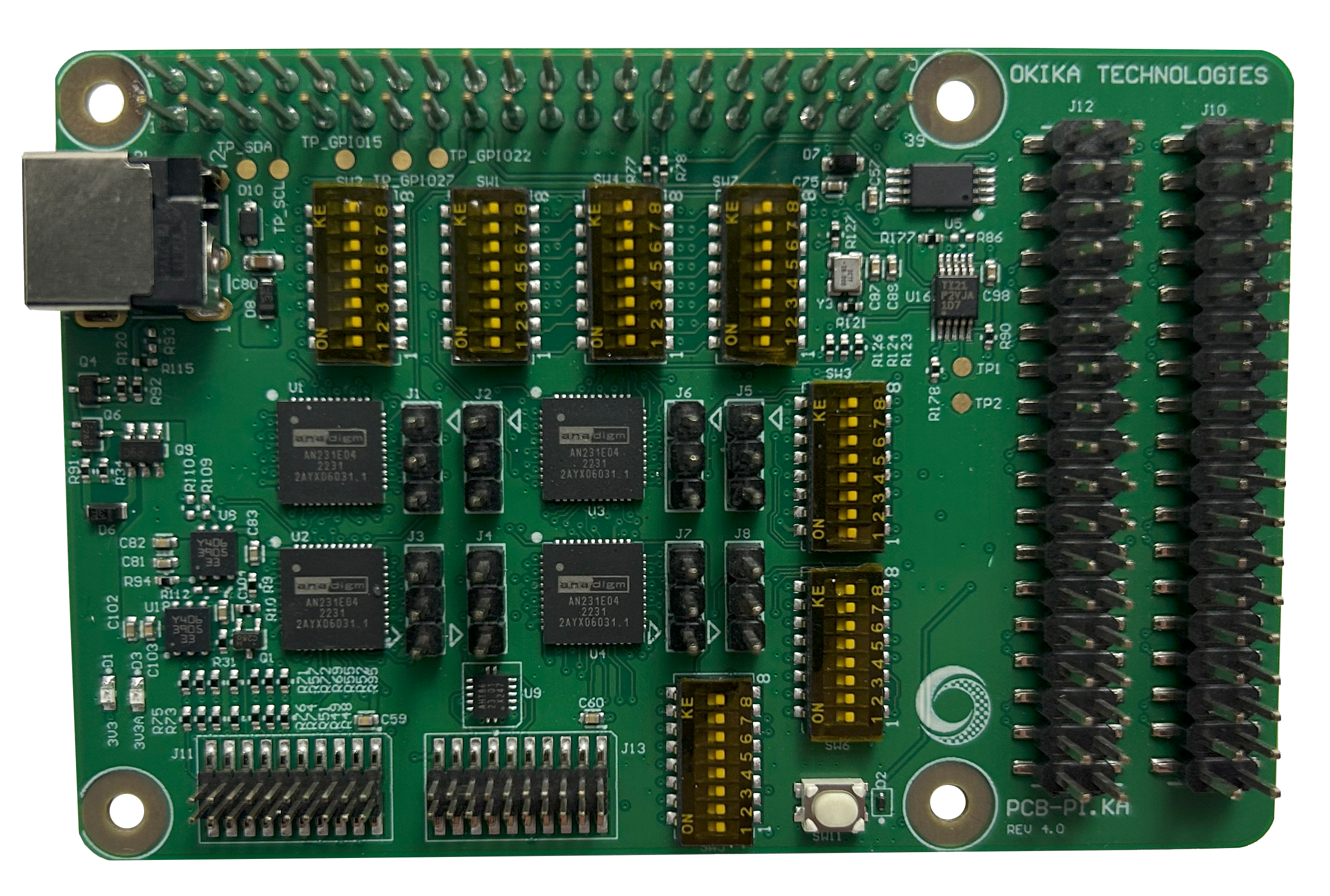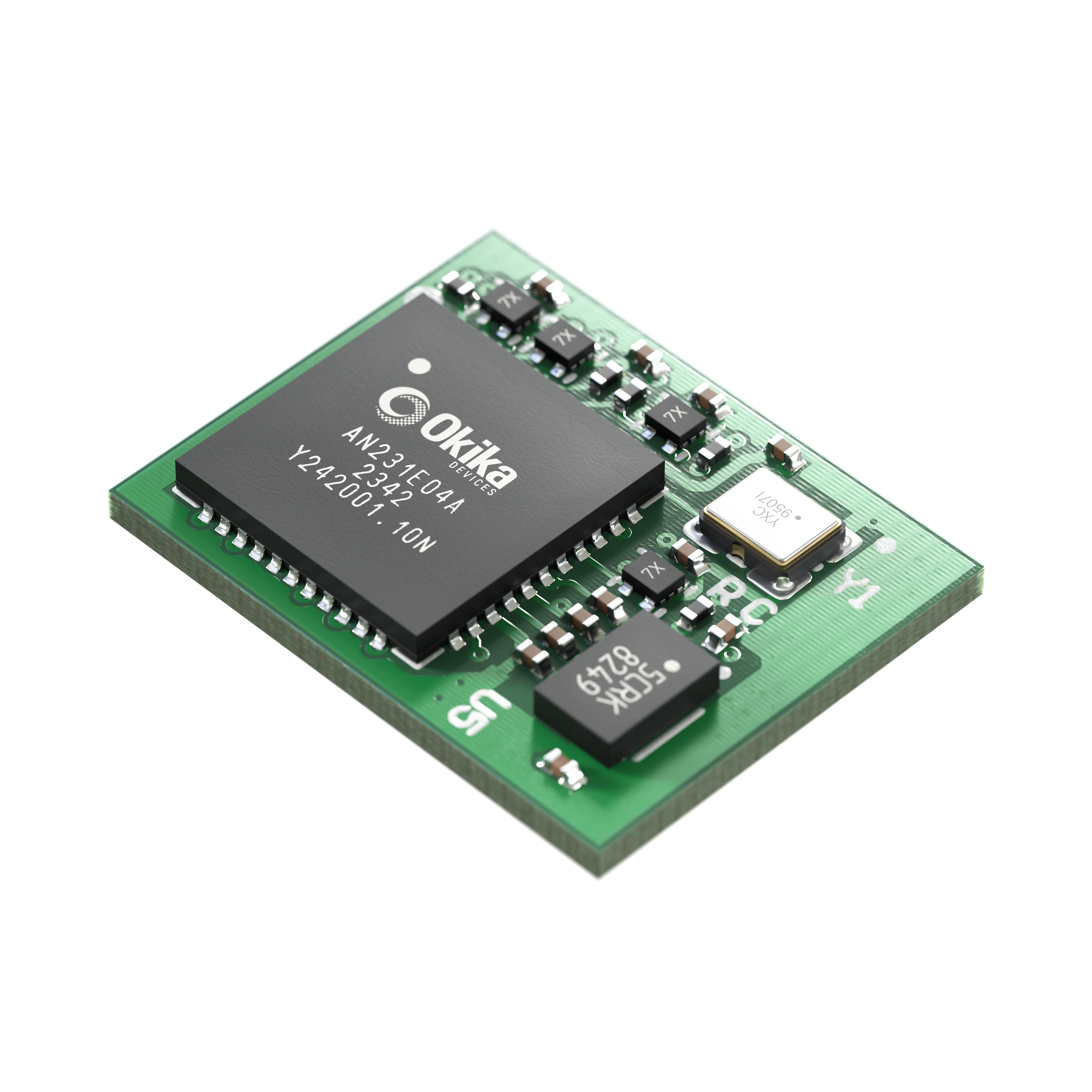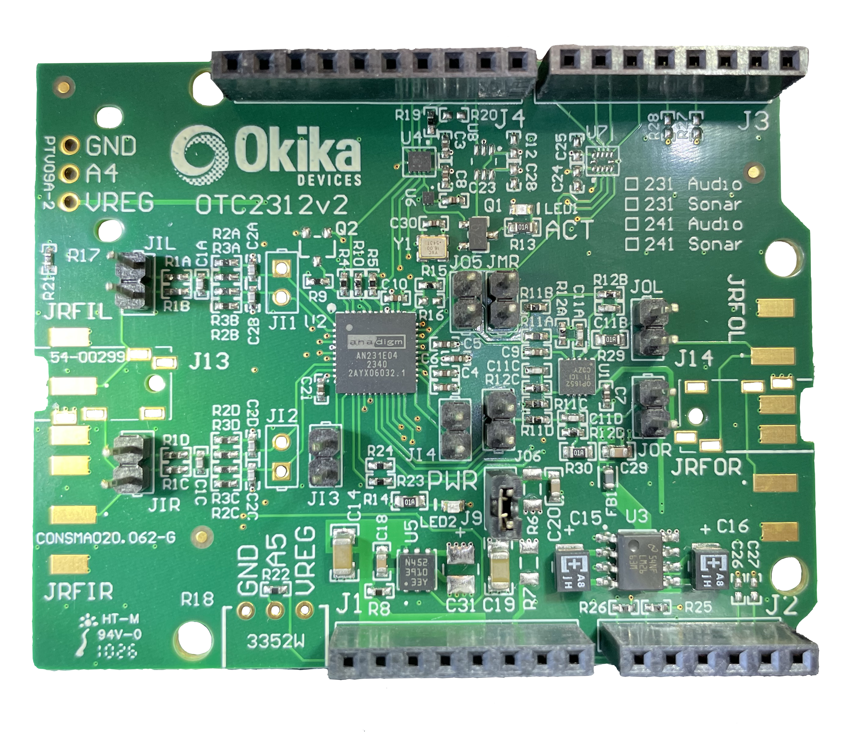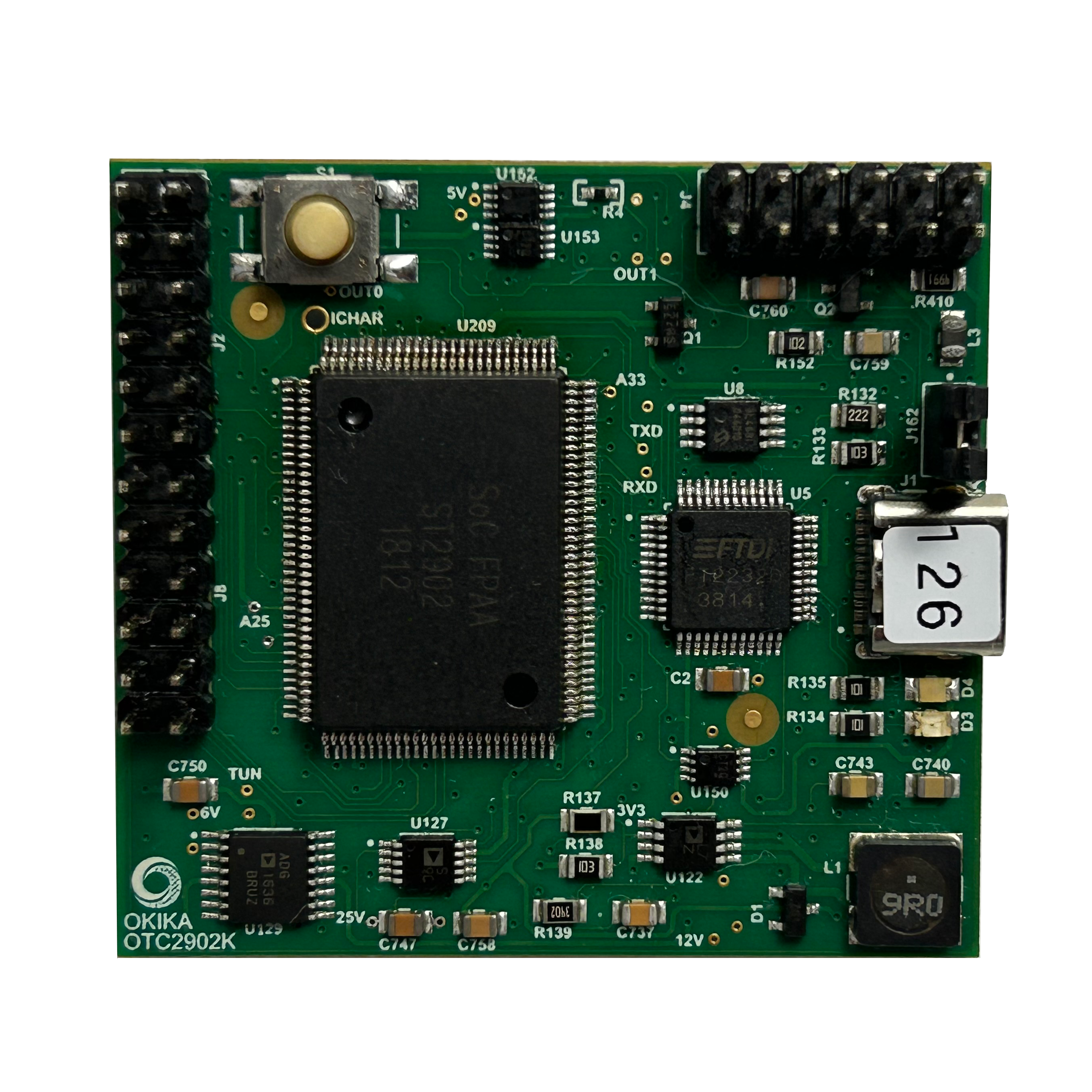

A field-programmable analog array, or FPAA, is an integrated circuit whose analog functions and signal paths can be configured after manufacturing. It brings software-controlled flexibility to functions that are traditionally built from fixed networks of amplifiers, resistors, capacitors, comparators, and switches. FPAA architectures vary across manufacturers and device families. This article explains the general principles using Okika’s AN2X1E04 FlexAnalog family as a representative example.
The comparison to an FPGA is useful but incomplete. An FPGA configures digital logic gates, registers, and routing. An FPAA configures real analog resources. Voltage, current, bandwidth, noise, phase, distortion, and headroom remain part of the design.
Understanding an FPAA therefore requires looking at five elements:
- Analog input and output cells
- Configurable Analog Blocks
- Configurable Analog Modules
- Programmable routing and clocks
- Configuration and dynamic reconfiguration
Analog I/O cells connect the device to the system
The I/O cells form the boundary between external signals and the internal analog array. Depending on the device and configuration, they may provide functions such as:
- Input and output buffering
- Differential or single-ended interfacing
- Level translation or reference control
- Filtering
- Signal routing to internal resources
- Connection to package pins
The I/O configuration must match the external source and load. A fully differential internal path may connect to a board that provides ground-referenced single-ended inputs and buffered outputs. The designer must understand where conversion between these formats occurs.
I/O cells are not simply wires. Their bandwidth, common-mode range, impedance, and optional functions affect the complete signal chain.
Configurable Analog Blocks provide physical resources
The core of an FPAA is an array of Configurable Analog Blocks, commonly called CABs. A CAB contains physical analog elements that can be connected and configured to implement different functions.
In the Okika AN2X1E04 family, each device includes four CABs and seven analog I/O cells. Across the device, available resources include operational amplifiers, comparators, successive-approximation logic elements, and a bank of matched programmable capacitors or switched capacitors.
These are real circuit elements. A configured amplifier uses an internal amplifier. A filter uses amplifier, capacitor, clock, and routing resources. The number and type of functions that fit in one device depend on the resources each function consumes.
This is similar to resource utilization in an FPGA, but analog fit is not measured only by logic count. A design may be limited by available op amps, capacitor ratios, clocks, I/O cells, routing, bandwidth, or internal signal range.
Configurable Analog Modules describe useful functions
Designers generally do not configure every switch and capacitor manually. FPAA design software provides higher-level functions known as Configurable Analog Modules, or CAMs.
CAMs can represent functions such as:
- Amplifiers
- Low-pass, high-pass, and band-pass filters
- Comparators
- Integrators and differentiators
- Oscillators
- Rectifiers
- Multipliers
- Signal converters
- Automatic gain-control elements
A CAM includes a user-facing parameter form and implementation rules. The designer selects the function and enters values such as gain, corner frequency, Q, polarity, or clock behavior. The software maps the requested function into physical CAB resources.
The requested value may be adjusted to a realizable value based on capacitor ratios, clock divisors, and device limits. Design reports and simulation should be reviewed to confirm the implemented result.
Programmable routing builds the signal chain
The analog blocks become a circuit through programmable interconnect. Routing connects I/O cells, CAM inputs and outputs, internal references, clocks, and other resources.
Routing flexibility allows one device to implement many topologies, but interconnect is not electrically invisible. Parasitic capacitance, switch resistance, loading, and signal swing influence real performance. Design software accounts for supported routing behavior, but good analog practice remains necessary.
Long or complex internal paths may reduce available bandwidth or increase sensitivity. The software may reject a placement when the required resources or valid routes are unavailable.
Clocks control switched-capacitor behavior
Many FPAA functions use switched-capacitor techniques. A clock controls charge transfer, creating effective resistances and time constants that depend on clock frequency and capacitor ratios.
Changing a clock divisor can change filter cutoff frequency, oscillator frequency, integration rate, or other time-dependent parameters. Several CAMs may share or use different internal clocks, so clock planning is a system-level part of the FPAA design.
The clock must be sufficiently faster than the processed signal. Clock feedthrough and sampled-data aliasing must also be considered. Input and output filtering, differential paths, supply decoupling, and layout affect the measured result.
Configuration data defines the circuit
Once the design is placed, routed, checked, and simulated, the software generates a digital configuration bitstream. That data controls internal switches, capacitor settings, clock selections, I/O behavior, and routing.
The configuration may be:
- Sent from a development tool
- Stored in nonvolatile memory
- Loaded by a microcontroller, FPGA, or other host
- Exported in a file format for an embedded system
After power-up or reset, the device receives a primary configuration. This establishes the circuit and device addressing required for later updates.
The host does not process the analog waveform by sending individual samples. It sends configuration data. Once configured, the analog circuit operates continuously in hardware.
Dynamic reconfiguration changes the circuit during operation
A dynamically reconfigurable FPAA can receive new configuration data while the current circuit continues to operate. In the AN2X1E04 architecture, new data can be loaded into shadow memory and transferred to the active analog array after loading is complete.
Reconfiguration can be partial or complete, depending on the device, generated data, and system design.
Parameter-level changes
The host may change a CAM parameter such as:
- Gain
- Filter corner frequency
- Comparator threshold
- Oscillator frequency
- Integration constant
Topology-level changes
The host may replace one analog function with another or alter routing, for example:
- Low-pass filter to band-pass filter
- Sensor channel A to sensor channel B
- Measurement mode to calibration mode
- Wide-band acquisition to narrow-band detection
Resource reuse
A circuit can be reconfigured at different points in a duty cycle. One set of analog resources can perform one function during a measurement interval and another function during calibration or standby.
This can reduce duplicated hardware, but the system must account for transition timing, output behavior, and any state that is lost during the change.
Static and dynamic configuration are different design problems
A statically configured FPAA is loaded once and operates as a fixed analog circuit until reset or power-down. This is useful for rapid prototyping, product variants, or factory configuration.
A dynamically configured system includes a host, state logic, timing requirements, and multiple verified analog states. The designer must specify:
- When new data is loaded
- What triggers activation
- How long the change takes
- Whether the output must be muted or ignored during transition
- How the ADC and downstream processor synchronize
- What happens if configuration data is interrupted or invalid
Dynamic behavior should be tested on hardware under the actual signal conditions.
What FPAAs can and cannot do
FPAAs are well suited to functions that map efficiently onto their available analog resources and bandwidth. These may include signal conditioning, filtering, gain control, comparison, waveform generation, control functions, and analog feature extraction.
They are not universal replacements for:
- High-voltage or high-current power circuits
- Very high-frequency RF signal chains beyond the device bandwidth
- Ultra-low-noise or ultra-high-precision circuits that exceed the architecture’s performance
- Large numerical algorithms requiring memory and arithmetic precision
- Every fixed-function analog IC
A fixed circuit may be smaller, lower noise, lower cost, or more precise when the requirement never changes. An FPAA is most valuable when reconfiguration, iteration speed, functional consolidation, or lifecycle adaptability offsets the programmable architecture’s constraints.
A practical FPAA design workflow
- Define input range, bandwidth, noise, and output requirements.
- Select the device and development board.
- Configure I/O cells.
- Place CAMs and set parameters.
- Connect the analog path.
- Review clocks and resource use.
- Simulate gain, frequency response, and transients.
- Check internal headroom and operating limits.
- Generate and load the configuration.
- Measure the hardware.
- Revise the circuit or add dynamic states.
- Export configuration data and documentation for the embedded system.
Programmable does not mean abstract
An FPAA makes analog hardware configurable, but it does not turn analog design into a purely digital exercise. The circuit still responds to source impedance, noise, grounding, power supplies, temperature, bandwidth, and signal amplitude.
The advantage is that engineers can work with those analog realities through a programmable platform. They can change the function, test alternatives, support multiple operating modes, and update the front end without replacing the entire board.